


| Develop Novel Mass Production Technique for Micro-LED Displays | |||||||
| Writer | 관리자 | ||||||
|---|---|---|---|---|---|---|---|
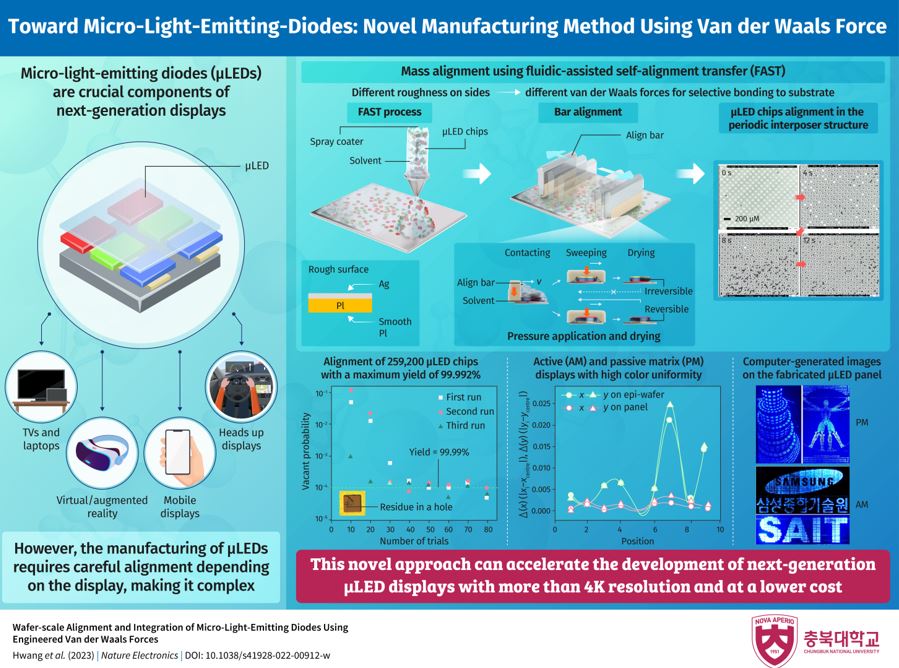
Image title: Fluid-Assisted Self-Alignment (FAST) for fabricating micro-LED displays Image caption: The FAST method ensures high accuracy and transfer yield and can also be used to develop high-resolution displays at low cost. It has the potential to sky-rocket the mass production of micro-LED displays. Image credit: Jaewook Jeong from Chungbuk National University License type: Original Content Usage restrictions: Cannot be reused without permission
The proposed fluid-assisted self-alignment technique can make the mass production of micro-LED displays easier and economical
Micro-light-emitting devices (μLEDs) are the ultimate evolution of display technology. Their mass production requires the mass transfer of many chips over large areas. However, these techniques often require additional alignment and modifications, increasing their complexity and cost. To address this, researchers from Korea have now developed a novel fluid-assisted self-alignment transfer method, which enables easier fabrication while also reducing cost. The proposed technology has the potential to propel the mass production of μLED displays. Micro-light-emitting-diodes (μLEDs) represent the next frontier in display technology, with applications ranging from energy-efficient mobile and heads-up displays to virtual and augmented reality devices, and even the next generation of televisions. A key technique used in the manufacturing of such μLED displays is the mass transfer of more than a million μLED chips over large areas with high accuracy, alignment speed, and minimal mid-production repair. However, this intricate process is still in the early stages of development, often requiring additional adjustments based on the specific device for which the display is intended. This makes the technique both cumbersome and costly, calling for other viable alternatives for manufacturing μLED displays.
To address this, a team of researchers from Korea, led by Professor Jaewook Jeong from the School of Information and Communication Engineering at Chungbuk National University, has introduced an innovative mass transfer technique, known as fluidic-assisted self-alignment transfer (FAST). “Considering the low aspect ratio and tiny mass combined with the sheer number of μLED chips, fluidic transfer could be a viable technique, provided that the two faces of the chips could be selectively aligned. Under fluid-mediated conditions, the dynamics of these chips are predominately affected by the van der Waals force, which is the attraction force between atoms. We rationalized that by manipulating these forces, the challenges associated with the mass transfer of μLED chips could be addressed” explains Prof. Jeong, while talking about the rationale behind this technique. The study detailing their groundbreaking approach was published in Volume 6, Issue 10 of the journal Nature Electronics on January 30, 2023.
At the core of the FAST process lies a unique principle—developing two distinct faces of the μLED chips, where one face exhibits a low van der Waals (vdW) force, while the other possesses a high vdW force. To achieve this, the team increased the surface roughness of one face by depositing silver, reducing the vdW force. The other face, being smooth and flat, was left untouched and exhibited a high vdW force. This difference in vdW force enables precise alignment of the chips on the substrates, with the high vdW force securing the chips to the substrate. Subsequently, the chips were immersed in a fluid to diminish the overall vdW forces of both surfaces, facilitating smooth movement towards their target. During this phase, a custom-designed align bar was utilized to apply the necessary force and dry the bottom face of the chips, increasing its vdW force and resulting in accelerated alignment and enhanced controllability.
Using this innovative method, the researchers achieved the alignment of approximately 259,200 μLED chips with an impressive accuracy rate of 100%, boasting a yield of 99.996% over 40 align bar trials. Notably, the probability of failure was reduced to a mere 0.01%, consistent with their theoretical calculations. To underscore the potential of this approach, the team applied the FAST method to develop both active matrix and passive matrix μLED displays. These displays showcased high colour uniformity, attributed to the random mixing effect of μLED chips in the fluid. Moreover, the technology holds promise for creating displays with large areas, exceeding 4k resolution, all while maintaining cost-effectiveness.
Highlighting the importance of developed FAST method, Prof. Jeong says, “In the future, displays will be ubiquitous. Instead of utilizing traditional OLED displays, the μLED displays will show clear, bright, and high-resolution moving images at a low cost across various display sizes, and we anticipate their use in various devices such as wearables, virtual and augmented reality displays, and even in large signage displays. The developed FAST method will be crucial for achieving cost-effective μLED displays that meets customer needs in the future.”
In conclusion, this innovative technology marks a significant stride toward advanced μLED displays, promising high definition, clarity, and cost-effectiveness.
Reference
About the Chungbuk National University Established in 1951 in Cheongju, South Korea, Chungbuk National University (CBNU) proudly stands as one of the ten Flagship Korean National Universities. Guided by the core values of Harmony, Dignity, and Future, CBNU envisions a dynamic future driven by the collaborative spirit of its vibrant community. Having produced over 150,000 graduates since its inception, its alumni actively contribute to societal development. Positioned advantageously at the heart of the nation, CBNU is celebrated for its central location—a key strength. Currently ranked first for student satisfaction nationwide, the university aspires to soar among the top 100 in Asia and the top 10 in Korea, embodying a commitment to excellence and progress.
About Professor Jaewook Jeong Jaewook Jeong is currently a Professor at the School of Information and Communication Engineering at Chungbuk National University. He received B.S. and M.S. degrees in Physics from Seoul National University, Seoul, South Korea, in 2003 and 2005, respectively. Subsequently, he received his Ph.D. in electrical engineering from the Seoul National University in 2009. His team’s research focus centres on the development of nano-micro device technology tailored for printed, flexible, and stretchable thin-film devices and the creation of displays and sensors designed for wearable and electronic applications.
|
|||||||
| Attachments | |||||||