


| MULTI-FUNCTIONAL NANOELECTRONICS LAB | |
  MULTI-FUNCTIONAL NANOELECTRONICS LAB
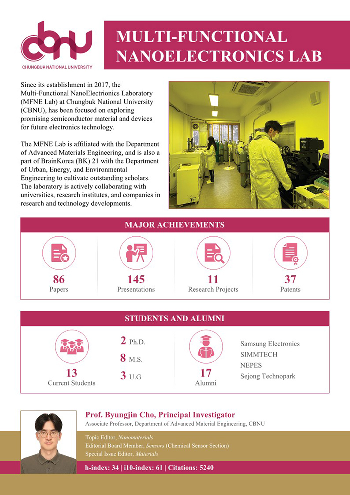
Since its establishment in 2017, the Multi-Functional NanoElectrionics Laboratory (MFNE Lab) at Chungbuk National University (CBNU), has been focused on exploring promising semiconductor material and devices for future electronics technology. The MFNE Lab is affiliated with the Department of Advanced Materials Engineering, and is also a part of BrainKorea (BK) 21 with the Department of Urban, Energy, and Environmental Engineering to cultivate outstanding scholars. The laboratory is actively collaborating with universities, research institutes, and companies in research and technology developments.
MAJOR ACHIEVEMENTS -86 Papers -145 Presentations -11 Research Projects -37 Patents
STUDENTS AND ALUMNI 13 Current Students -2 Ph.D. -8 M.S. -3 U.G 17 Alumni -Samsung Electronics -SIMMTECH -NEPES -Sejong Technopark
Prof. Byungjin Cho, Principal Investigator Associate Professor, Department of Advanced Material Engineering, CBNU Topic Editor, Nanomaterials Editorial Board Member, Sensors (Chemical Sensor Section) Special Issue Editor, Materials h-index: 34 | i10-index: 61 | Citations: 5240
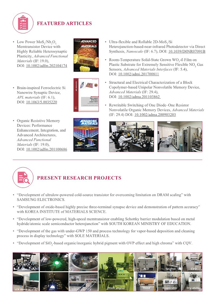
FEATURED ARTICLES • Low Power MoS2 /Nb2 O5 Memtransistor Device with Highly Reliable Heterosynaptic Plasticity, Advanced Functional Materials (IF: 19.0), DOI: 10.1002/adfm.202104174 • Brain-inspired Ferroelectric Si Nanowire Synaptic Device, APL materials (IF: 6.1), DOI: 10.1063/5.0035220 • Organic Resistive Memory Devices: Performance Enhancement, Integration, and Advanced Architectures, Advanced Functional Materials (IF: 19.0), DOI: 10.1002/adfm.201100686 • Ultra-flexible and Rollable 2D-MoS2 /Si Heterojunction-based-near-infrared Photodetector via Direct Synthesis, Nanoscale (IF: 6.7), DOI: 10.1039/D0NR07091B • Room-Temperature Solid-State Grown WO3 -б Film on Plastic Substrate for Extremely Sensitive Flexible NO2 Gas Sensors, Advanced Materials Interfaces (IF: 5.4), DOI: 10.1002/admi.201700811 • Structural and Electrical Characterization of a Block Copolymer-based Unipolar Nonvolatile Memory Device, Advanced Materials (IF: 29.4), DOI: 10.1002/adma.201103862 • Rewritable Switching of One Diode–One Resistor Nonvolatile Organic Memory Devices, Advanced Materials (IF: 29.4) DOI: 10.1002/adma.200903203
PRESENT RESEARCH PROJECTS • “Development of ultralow-powered cold-source transistor for overcoming limitation on DRAM scaling” with SAMSUNG ELECTRONICS. • “Development of oxide-based highly precise three-terminal synapse device and demonstration of pattern accuracy” with KOREA INSTITUTE of MATERIALS SCIENCE. • “Development of low-powered, high-speed memtransistor enabling Schottky barrier modulation based on metal hydride/atomic scale semiconductor heterojunction” with SOUTH KOREAN MINISTRY OF EDUCATION. • “Development of the gas with under-GWP 150 and process technology for vapor-based deposition and cleaning process in display technology” with SOLE MATERIALS. • “Development of SiO2 -based organic/inorganic hybrid pigment with OVP effect and high chroma” with CQV.
|